- 您现在的位置:买卖IC网 > Sheet目录3874 > PIC16LF724-E/PT (Microchip Technology)IC PIC MCU FLASH 7KB 44-TQFP
PIC16F72X/PIC16LF72X
DS41341E-page 10
2009 Microchip Technology Inc.
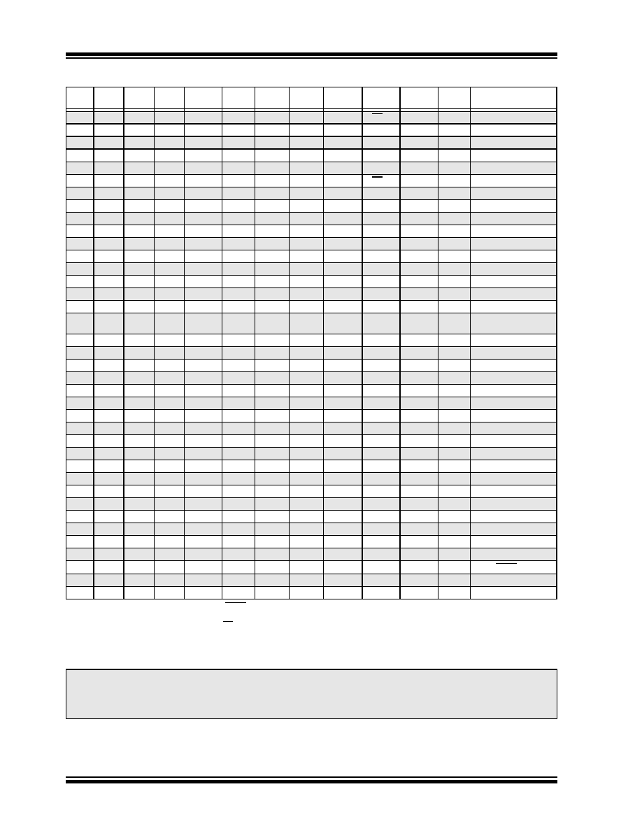
TABLE 2:
40/44-PIN PDIP/TQFP/QFN SUMMARY (PIC16F724/727/PIC16LF724/727
)
I/O
40-Pin
PDIP
44-Pin
TQFP
44-Pin
QFN
A/D
Cap
Sensor
Timers
CCP
AUSART
SSP
Interrupt
Pull-Up
Basic
RA0
2
19
AN0
—
SS(3)
—
VCAP(4)
RA1
3
20
AN1
—
RA2
4
21
AN2
—
RA3
5
22
AN3/VREF
——
—
RA4
6
23
—
CPS6
T0CKI
—
RA5
7
24
AN4
CPS7
—
SS(3)
——
VCAP(4)
RA6
14
31
33
—
OSC2/CLKOUT/VCAP(4)
RA7
133032
—
OSC1/CLKIN
RB0
33
8
9
AN12
CPS0
—
IOC/INT
Y
—
RB1
34
9
10
AN10
CPS1
—
IOC
Y
—
RB2
35
10
11
AN8
CPS2
—
IOC
Y
—
RB3
36
11
12
AN9
CPS3
—
CCP2(2)
—
IOC
Y
—
RB4
37
14
AN11
CPS4
—
IOC
Y
—
RB5
381515
AN13
CPS5
T1G
—
IOC
Y
—
RB6
39
16
—
IOC
Y
ICSPCLK/ICDCLK
RB7
40
17
—
IOC
Y
ICSPDAT/ICDDAT
RC0
15
32
34
—
T1OSO/
T1CKI
—
RC1
16
35
—
T1OSI
CCP2(2)
——
—
RC2
17
36
—
CCP1
—
RC3
18
37
—
SCK/SCL
—
RC4
23
42
—
SDI/SDA
—
RC5
24
43
—
SDO
—
RC6
25
44
—
TX/CK
—
RC7
26
1
—
RX/DT
—
RD0
19
38
—
CPS8
—
RD1
20
39
—
CPS9
—
RD2
21
40
—
CPS10
—
RD3
22
41
—
CPS11
—
RD4
27
2
—
CPS12
—
RD5
28
3
—
CPS13
—
RD6
29
4
—
CPS14
—
RD7
30
5
—
CPS15
—
RE0
8
25
AN5
—
RE1
9
26
AN6
—
RE2
10
27
AN7
—
RE3
1
18
—
Y(1)
MCLR/VPP
—
11,32
7,20
7,8,28
—
VDD
—
12,13
6,29
6,30,31
—
VSS
Note
1:
Pull-up enabled only with external MCLR configuration.
2:
RC1 is the default pin location for CCP2. RB3 may be selected by changing the CCP2SEL bit in the APFCON register.
3:
RA5 is the default pin location for SS. RA0 may be selected by changing the SSSEL bit in the APFCON register.
4:
PIC16F72X devices only.
Note:
The PIC16F72X devices have an internal low dropout voltage regulator. An external capacitor must be
connected to one of the available VCAP pins to stabilize the regulator. For more information, see
Section 5.0 “Low Dropout (LDO) Voltage Regulator”. The PIC16LF72X devices do not have the voltage
regulator and therefore no external capacitor is required.
发布紧急采购,3分钟左右您将得到回复。
相关PDF资料
PIC18LF44J10T-I/ML
IC PIC MCU FLASH 8KX16 44QFN
PIC16LF727-I/PT
IC PIC MCU FLASH 8K 1.8V 44-TQFP
PIC24F08KA102-I/SO
IC PIC MCU FLASH 8K 28-SOIC
PIC18LF44J10T-I/PT
IC PIC MCU FLASH 8KX16 44TQFP
PIC24F16KL401-I/SO
IC MCU 16BIT 16KB FLASH 20-SOIC
PIC18LF25J10T-I/SS
IC PIC MCU FLASH 16KX16 28-SSOP
PIC16LF1527-I/PT
MCU PIC 28KB FLASH 64TQFP
PIC18F25K20-I/SP
IC PIC MCU FLASH 16KX16 28-DIP
相关代理商/技术参数
PIC16LF724-I/ML
功能描述:8位微控制器 -MCU 7KB Flash Prog 16MHz Int Osc 1.8V-5.5V
RoHS:否 制造商:Silicon Labs 核心:8051 处理器系列:C8051F39x 数据总线宽度:8 bit 最大时钟频率:50 MHz 程序存储器大小:16 KB 数据 RAM 大小:1 KB 片上 ADC:Yes 工作电源电压:1.8 V to 3.6 V 工作温度范围:- 40 C to + 105 C 封装 / 箱体:QFN-20 安装风格:SMD/SMT
PIC16LF724-I/MV
功能描述:8位微控制器 -MCU 7KB Flash RAM 192b nanoWatt RoHS:否 制造商:Silicon Labs 核心:8051 处理器系列:C8051F39x 数据总线宽度:8 bit 最大时钟频率:50 MHz 程序存储器大小:16 KB 数据 RAM 大小:1 KB 片上 ADC:Yes 工作电源电压:1.8 V to 3.6 V 工作温度范围:- 40 C to + 105 C 封装 / 箱体:QFN-20 安装风格:SMD/SMT
PIC16LF724-I/P
功能描述:8位微控制器 -MCU 7KB 1.8-3.6V 16MHz 8b ADC CCP Lo Pwr
RoHS:否 制造商:Silicon Labs 核心:8051 处理器系列:C8051F39x 数据总线宽度:8 bit 最大时钟频率:50 MHz 程序存储器大小:16 KB 数据 RAM 大小:1 KB 片上 ADC:Yes 工作电源电压:1.8 V to 3.6 V 工作温度范围:- 40 C to + 105 C 封装 / 箱体:QFN-20 安装风格:SMD/SMT
PIC16LF724-I/PT
功能描述:8位微控制器 -MCU 7KB 1.8-3.6V 16MHz 8b ADC CCP Lo Pwr
RoHS:否 制造商:Silicon Labs 核心:8051 处理器系列:C8051F39x 数据总线宽度:8 bit 最大时钟频率:50 MHz 程序存储器大小:16 KB 数据 RAM 大小:1 KB 片上 ADC:Yes 工作电源电压:1.8 V to 3.6 V 工作温度范围:- 40 C to + 105 C 封装 / 箱体:QFN-20 安装风格:SMD/SMT
PIC16LF724T-I/ML
功能描述:8位微控制器 -MCU 7KB Flash Prog 16MHz Int Osc 1.8V-5.5V
RoHS:否 制造商:Silicon Labs 核心:8051 处理器系列:C8051F39x 数据总线宽度:8 bit 最大时钟频率:50 MHz 程序存储器大小:16 KB 数据 RAM 大小:1 KB 片上 ADC:Yes 工作电源电压:1.8 V to 3.6 V 工作温度范围:- 40 C to + 105 C 封装 / 箱体:QFN-20 安装风格:SMD/SMT
PIC16LF724T-I/MV
功能描述:8位微控制器 -MCU 7KB Flash RAM 192b nanoWatt RoHS:否 制造商:Silicon Labs 核心:8051 处理器系列:C8051F39x 数据总线宽度:8 bit 最大时钟频率:50 MHz 程序存储器大小:16 KB 数据 RAM 大小:1 KB 片上 ADC:Yes 工作电源电压:1.8 V to 3.6 V 工作温度范围:- 40 C to + 105 C 封装 / 箱体:QFN-20 安装风格:SMD/SMT
PIC16LF724T-I/PT
功能描述:8位微控制器 -MCU 7KB Flash Prog 16MHz Int Osc 1.8V-5.5V
RoHS:否 制造商:Silicon Labs 核心:8051 处理器系列:C8051F39x 数据总线宽度:8 bit 最大时钟频率:50 MHz 程序存储器大小:16 KB 数据 RAM 大小:1 KB 片上 ADC:Yes 工作电源电压:1.8 V to 3.6 V 工作温度范围:- 40 C to + 105 C 封装 / 箱体:QFN-20 安装风格:SMD/SMT
PIC16LF726-E/ML
功能描述:8位微控制器 -MCU 14KBFlash Prog 16MHz Int Osc 1.8V-5.5V
RoHS:否 制造商:Silicon Labs 核心:8051 处理器系列:C8051F39x 数据总线宽度:8 bit 最大时钟频率:50 MHz 程序存储器大小:16 KB 数据 RAM 大小:1 KB 片上 ADC:Yes 工作电源电压:1.8 V to 3.6 V 工作温度范围:- 40 C to + 105 C 封装 / 箱体:QFN-20 安装风格:SMD/SMT